
Table of Contents
What is an Operational Amplifier?
An operational amplifier (op amp) is an analog circuit block that takes a differential voltage input and produces a single-ended voltage output.
Op amps usually have three terminals: two high-impedance inputs and a low-impedance output port. The inverting input is denoted with a minus (-) sign, and the non-inverting input uses a positive (+) sign. Operational amplifiers work to amplify the voltage differential between the inputs, which is useful for a variety of analog functions including signal chain, power, and control applications.
Operational Amplifier Clasifications
There are four ways to classify operational amplifiers:
- Voltage amplifiers take voltage in and produce a voltage at the output.
- Current amplifiers receive a current input and produce a current output.
- Transconductance amplifiers convert a voltage input to a current output.
- Transresistance amplifiers convert a current input and produces a voltage output.
Because most op amps are used for voltage amplification, this article will focus on voltage amplifiers.
Operational Amplifiers: Key Characteristics and Parameters
There are many different important characteristics and parameters related to op amps (see Figure 1). These characteristics are described in greater detail below.
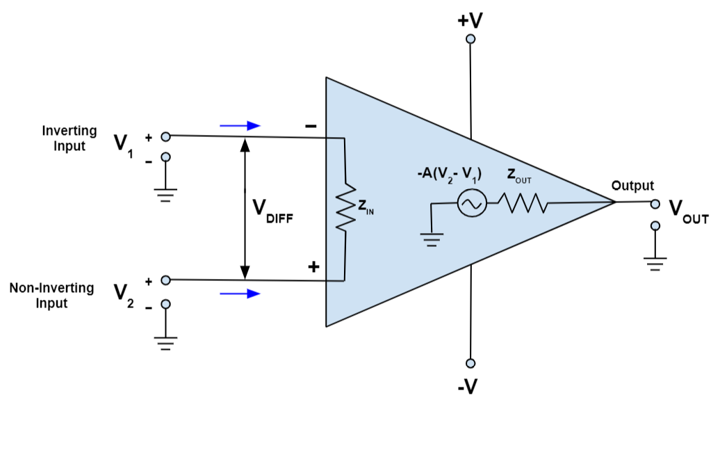
Open-loop gain
Open-loop gain: The open-loop gain (“A” in Figure 1) of an operational amplifier is the measure of the gain achieved when there is no feedback implemented in the circuit. This means the feedback path, or loop, is open. An open-loop gain often must be exceedingly large (10,000+) to be useful in itself, except with voltage comparators.
Voltage comparators compare the input terminal voltages. Even with small voltage differentials, voltage comparators can drive the output to either the positive or negative rails. High open-loop gains are beneficial in closed-loop configurations, as they enable stable circuit behaviors across temperature, process, and signal variations.
Input impedance
Another important characteristic of op amps is that they generally have high input impedance (“ZIN” in Figure 1). Input impedance is measured between the negative and positive input terminals, and its ideal value is infinity, which minimizes loading of the source. (In reality, there is a small current leakage.) Arranging the circuitry around an operational amplifier may significantly alter the effective input impedance for the source, so external components and feedback loops must be carefully configured. It is important to note that input impedance is not solely determined by the input DC resistance. Input capacitance can also influence circuit behavior, so that must be taken into consideration as well.
Output impedance
An operational amplifier ideally has zero output impedance (“ZOUT” in Figure 1). However, the output impedance typically has a small value, which determines the amount of current it can drive, and how well it can operate as a voltage buffer.
Frequency response and bandwidth (BW)
An ideal op amp would have an infinite bandwidth (BW) and would be able to maintain a high gain regardless of signal frequency. However, all operational amplifiers have a finite bandwidth, generally called the “-3dB point,” where the gain begins to roll as frequency increases. The gain of the amplifier then decreases at a rate of -20dB/decade while the frequency increases. Op amps with a higher BW have improved performance because they maintain higher gains at higher frequencies; however, this higher gain results in larger power consumption or increased cost.
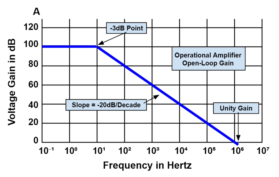
Gain bandwidth product (GBP)
As the name suggests, GBP is a product of the amplifier’s gain and bandwidth. GBP is a constant value across the curve, and can be calculated with Equation (1):
GBP is measured at the frequency point at which the operational amplifier’s gain reaches unity. This is useful because it allows the user to calculate the device’s open-loop gain at different frequencies. An operational amplifier’s GBP is generally a measure of its usefulness and performance, as op amps with a higher GBP can be used to achieve better performance at higher frequencies.
These are the major parameters to consider when selecting an operational amplifier in your design, but there are many other considerations that may influence your design, depending on the application and performance needs. Other common parameters include input offset voltage, noise, quiescent current, and supply voltages.
Negative Feedback and Closed-Loop Gain
In an operational amplifier, negative feedback is implemented by feeding a portion of the output signal through an external feedback resistor and back to the inverting input (see Figure 3).
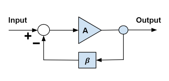
Negative feedback is used to stabilize the gain. By using a negative feedback, the closed-loop gain can be determined via external feedback components that can have higher accuracy compared to the operational amplifier’s internal components. This is because the internal op amp components may vary substantially due to process shifts, temperature changes, voltage changes, and other factors. The closed-loop gain can be calculated with Equation (2):
Operational Amplifiers: Advantages and Limitations
There are many advantages to using an operational amplifier. Operational amplifiers often come in the form of an IC, and are widely available, with countless selectable performance levels to meet every application’s needs. Op amps have a broad range of usages, and as such are a key building block in many analog applications — including filter designs, voltage buffers, comparator circuits, and many others. In addition, most companies provide simulation support, such as PSPICE models, for designers to validate their operational amplifier designs before building real designs.
The limitations to using operational amplifiers include the fact they are analog circuits, and require a designer that understands analog fundamentals such as loading, frequency response, and stability. It is not uncommon to design a seemingly simple op amp circuit, only to turn it on and find that it is oscillating. Due to some of the key parameters discussed earlier, the designer must understand how those parameters play into their design, which typically means the designer must have a moderate to high level of analog design experience.
Hi, I’m Vivek, a Senior Embedded Innovation Specialist. I have been working on Embedded Systems and IoT for the past 11 years. I love to share my knowledge and train those who are interested. Nerdyelectronics.com was started out of this interest. You can read my full profile in this link.


