Embedded Systems Learning Path Part 48 of 129 — View Full Path →
KEY TAKEAWAYS
A transistor can switch high-current loads (motors, relays) using a low-current control signal from a microcontroller
NPN transistors switch the ground path; PNP transistors switch the supply path
A base resistor limits current from the control pin; calculate it based on load current and transistor gain
A flyback diode across inductive loads (motors, relays) protects the transistor from voltage spikes
In this tutorial I will show how to use a transistor as a switch. Switching and Amplification are the most common application of a transistor and transistor is used as a switch in many digital circuits. Using transistor as a switch, we can use a small voltage level to control a bigger voltage level. For example, using 3.3v or 5v, we can control 12v or even 250v.Before moving forward we have to understand the operating modes of a transistor.
Operating Modes of a Transistor
Based on the biasing conditions transistor mainly operates in three regions namely cutoff, active and saturation regions.
Active Mode
When transistor is in active mode then it can be used as a current amplifier. In active mode of a transistor emitter-base junction should be forward biased and collector-base junction should be reverse biased as shown below. In active mode the current flows between emitter and collector and amount of current flow is proportional to the base current.
Saturation Mode
In Saturation mode both emitter-base and collector-base junctions are forward biased as shown below. Here, the transistor acts as a constant current source and transistor is completely switched ON. In this mode, the transistor acts almost as a short circuit. We will use this mode of the transistor to use it as a switch.
Cutoff Mode
In this mode, both emitter-base and collector-base junctions are reverse biased.in this mode transistor is completely switched off as a result current flowing through the transistor is zero.Hence, from above discussion, it is clear that transistor can be made to work as ON / OFF switch by operating transistor in cuttoff and saturation regions. This type of switching application can be used in digital electronics and also in domestic applications.
Transistor as a Switch
Both NPN and PNP transistors can be used as switch. In this section we will see how to use both of them in both active high and active low cases.
NPN Transistor as a Switch
The transistor operation can be performed by applying some voltage at base terminal. When some voltage (above threshold voltage i.e. Vin > 0.7 V) is applied between Base and Emitter then transistor will be in ON condition hence the collector current Vcc/Rc flows through the transistor. Therefore act as a short circuit and collector to emitter voltage is approximately equal to zero.Similarly, when Vin=0v or no input voltage is applied at the input of the transistor then transistor operates in cuttoff region and hence transistor acts as an open circuit and hence collector to emitter voltage is equal to the bias voltage of the transistor.
Implementation
Assume beta value of transistor to be 100 base resistance Rb= 1k ohm and collector resistance Rc=300 ohm, even you can select any value but always select resistor value such that Rb >> Rc as we need only a small base current to perform the operation. At the base a DC source is used and we are going to see the output at the collector by varying input voltage at two states i.e. 0v and 5v as shown in the fig.
NPN Transistor as a Switch
When, Vin > 0.7 v (Transistor in ON state)We get Ic = Vcc/Rc and Vce=0.Ic=5v/330 ohm = 15.1mATherefore, Base current Ib= Ic / βIb=151.5 µAFrom the above calculation, maximum value of collector current in the circuit is 15.1 mA when Vce=0v and corresponding base current is 151.5 µA. Therefore, when base current is increased beyond 151.5 µA then transistor will go in saturation state.When, Vin<0.7v (Transistor in Off State)We get Ib=0 and Ic=0Vce=Vcc-IcRc=5v – 0 = 5vWhen Input voltage applied is 5v, then the base current can be found using Kirchhoff’s voltage law.When Vin=5vIb = (Vin – Vbe)/Rb (Vbe=0.7V for Si transistor)Ib = (5V – 0.7)/1000 = 4.3 mAWhich is greater than 151.5 µA Therefore, transistor is driven to saturation state. Thus output at the collector becomes Approximately 0V.It is also possible to operate the relay using transistor. The transistor can energize the coil of the relay so that the external load connected to it can be controlled as shown below.
NPN Transistor Operating External Load Using Relay
In inductive loads, particularly switching of motors and inductors, sudden removal of power can keep a high potential across the coil. This high voltage can cause considerable damage to the rest circuit. Therefore, we have to use the diode in anti-parallel with inductive load to protect the circuit from induced voltages of the inductive load.
NPN transistor switch configurations:
There are mainly two configurations of NPN transistor as a switch, they are
Active High
Active Low
Active High
Whenever the Relay is in series with NPN transistor, then the circuit will become Active High input Circuit i.e. Vin >0.7V at this condition relay will get operated and external load is powered as shown in the figure.Note: In series configuration the relay can be at emitter side or may be at collector side but it is preferred to have the load at the collector side.
Active low
Whenever the Relay is in parallel with NPN transistor, then the circuit will become Active Low input Circuit i.e. Vin <= 0.7V at this condition relay will get operated and external load is powered as shown in the figure.
Active Low Configuration with relay parallel to NPN transistor
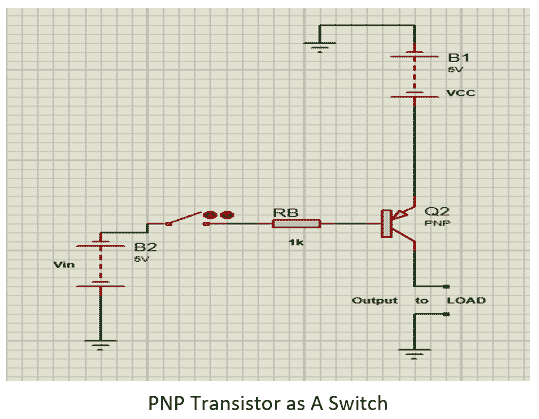
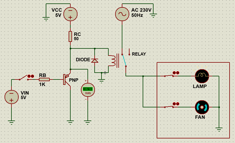
PNP transistor as SwitchSimilar to The NPN transistor, PNP transistor can also act as a switch, but in this case the emitter is connected to Constant voltage and collector is connected to ground through load as shown in the figure below.In this configuration base is always negatively biased with respect to emitter . So, the voltage Vbe is negative. Therefore, for conduction of PNP transistor emitter must be more positive with respect to both collector and base. You can see in the figure that the base is connected to negative terminal of the battery and emitter is connected to positive terminal of the battery. It is also possible to operate the relay to drive external load using PNP transistor. The transistor can energize the coil of the relay so that the external load connected to it can be controlled as shown below. NPN Transistor Operating External Load Using RelayIn inductive loads, particularly switching of motors and inductors, sudden removal of power can keep a high potential across the coil. This high voltage can cause considerable damage to the rest circuit. Therefore, we have to use the diode in anti-parallel with inductive load to protect the circuit from induced voltages of the inductive load.
PNP transistor switch configurations:
Similar to NPN ,PNP Transistor Switch also have two configurations of a switch, they are
Active High
Active Low
Active High
Whenever the Relay is in Parallel with PNP transistor, then the circuit will become Active High input Circuit. In this condition, relay will get operated and external load is powered when a high input is given into the base of the transistor, as shown in the image below.Active High Configuration with relay parallel to PNP transistor
Active low
Whenever the Relay is in series with PNP transistor, then the circuit will become Active Low input Circuit i.e. Vin <= – 0.7V at this condition relay will get operated and external load is powered as shown in the figure.(Note: In series configuration the relay can be at emitter side or may be at collector side) You can also watch this video on the working of Transistor as a switch.
Vivek Bhageria — Lead Firmware R&D Engineer, 12+ years. Ex-Bosch (automotive powertrain), MusicTribe (real-time audio), medical devices. M.Tech BITS Pilani. I write at NerdyElectronics — practical, register-level embedded systems for engineers who want to understand what’s actually happening under the hood.